Navigation Menu
Search code, repositories, users, issues, pull requests..., provide feedback.
We read every piece of feedback, and take your input very seriously.

Saved searches
Use saved searches to filter your results more quickly.
To see all available qualifiers, see our documentation .
- Notifications You must be signed in to change notification settings
This project discusses the design of an 8-bit asynchronous successive approximation register (SAR) analog-to-digital converter (ADC) implemented in 45nm CMOS technology.
muhammadaldacher/Analog-Design-of-Asynchronous-SAR-ADC
Folders and files.
| Name | Name | |||
|---|---|---|---|---|
| 8 Commits | ||||
Repository files navigation
Analog-design-of-asynchronous-sar-adc.
This project is about the design process of an 8-bit asynchronous successive approximation register (SAR) analog-to-digital converter (ADC) using 45nm CMOS technology. SAR ADCs are attractive circuits for applications that require low power with medium resolution and medium speed like in computing-in-memory cores for AI applications and in sensors for biomedical applications. The asynchronous architecture allow the ADC to operate without the need for an oversampled clock reducing the design complexities associated with higher frequencies. The top-level block diagram of the asynchronous SAR ADC is shown below, along with the timing diagram of the important signals.

1) Internal Clock Generator
The internal clock generator is the block responsible for providing the rest of the system with the clock signals to operate. This block produces 2 output signals, “clk_sample” and “clk_sar”, and receives 3 inputs “clk_ext”, “Ready”, and “EOC”.
2) Bootstrapped Sample-And-Hold Switches
The sample-and-hold circuit is basically a switch that captures the value of an analog signal at a certain moment and holds it constant for a certain amount of time. The bootstrapped switch help mitigate some of the switch non-idealities by keeping the switch’s VGS fixed during the sampling phase.
3) Capacitive DAC
The capacitive DAC uses charge redistribution to convert the digital code coming from the SAR logic into the corresponding analog voltage level to be compared by the comparator.
4) Dynamic Comparator
The comparator’s function is to compare the analog input levels coming from the DAC and to produce a digital output bit (either high or low) representing the result of the comparison. A high-speed low-power strongarm comparator is used.
5) SAR Logic
The SAR logic generates the digital code for the DAC in each comparison stage. At the end of the conversion cycle, the final digital code is outputted by an output register. The flipflops used are TSPC flipflops with asynchronous set and reset inputs.
* Analysis & Results:

Key References:
[1] O. Kardonik, "A study of SAR ADC and implementation of 10-bit asynchronous design," M.S. Thesis, Department of Electrical and Computer Engineering, University of Texas at Austin, 2013.
[2] P. J. A. Harpe et al., "A 26 uW 8 bit 10 MS/s Asynchronous SAR ADC for Low Energy Radios," IEEE Journal of Solid-State Circuits, vol. 46, no. 7, pp. 1585-1595, July 2011.
[3] M. Al-Qadasi, A. Alshehri, A. S. Almansouri, T. Al-Attar, and H. Fariborzi, "A High Speed Dynamic StrongARM Latch Comparator," 2018 IEEE 61st International Midwest Symposium on Circuits and Systems (MWSCAS), Windsor, ON, Canada, 2018, pp. 540-541.
[4] M. Dessouky and A. Kaiser, "Very low-voltage digital-audio Δ∑ modulator with 88-dB dynamic range using local switch bootstrapping," IEEE Journal of Solid-State Circuits, vol. 36, no. 3, pp. 349-355, March 2001.
For more info, check the project's report & ppt: https://github.com/muhammadaldacher/Analog-Design-of-Asynchronous-SAR-ADC/blob/main/%5BReport%5D%20Design%20of%20a%20Low-Power%20Asynchronous%20SAR%20ADC%20in%2045%20nm%20CMOS%20Technology.pdf
https://github.com/muhammadaldacher/Analog-Design-of-Asynchronous-SAR-ADC/blob/main/%5BPPT%5D%20Design%20of%20a%20Low-Power%20Asynchronous%20SAR%20ADC%20in%2045%20nm%20CMOS%20Technology.pdf
My project on google drive: https://drive.google.com/drive/folders/1zEzuneabBBtgcV0V-nYb4Kvp_cLarDpZ?usp=sharing
SAR ADCs Design and Calibration in Nano-scaled Technologies
The rapid progress of scaling and integration of modern complimentary metal oxide semiconductor (CMOS) technology motivates the replacement of traditional analog signal processing by digital alternatives. Thus, analog-to-digital converters (ADCs), as the interfaces between the analog world and the digital one, are driven to enhance their performance in terms of speed, resolution and power efficiency. However, in the presence of imperfections of device mismatch, thermal noise and reduced voltage headroom, efficient ADC design demands new strategies for design, calibration and optimization. Among various ADC architectures, successive-approximation-register (SAR) ADCs have received renewed interest from the design community due to their low hardware complexity and scaling-friendly property. However, the conventional SAR architecture has many limitations for high-speed, high-resolution applications. Many modified SAR architectures and hybrid SAR architectures have been reported to break the inherent constraints in the conventional SAR architecture. Loop-unrolled (LU) SAR ADCs have been recognized as a promising architecture for high-speed applications. However, mismatched comparator offsets introduce input-level dependent errors to the conversion result, which deteriorates the linearity and limits the resolution and the resolution of most reported SAR ADCs of this kind are limited to 6 bits. Also, for high-resolution SAR ADCs, the comparator noise specification is very stringent, which imposes a limitation on ADC speed and power-efficiency. Lastly, capacitor mismatch is an important limiting factor for SAR ADC linearity, and generally requires dedicated calibration to achieve efficient designs in terms of power and area. In this work, we investigate the impacts of offset mismatch, comparator noise and capacitor mismatch on high-speed SAR ADCs. An analytical model is proposed to estimate the resolution and predict the yield of LU-SAR ADCs with presence of comparator offset mismatch. A background calibration technique is proposed for resolving the comparator mismatch issue. A 150-MS/s 8-bit LU-SAR ADC is fabricated in a 130-nm CMOS technology to validate the concept. The measured result shows that the calibration improves the SNDR from 33.7-dB to 42.9-dB. The ADC consumes 640 μW from a 1.2 V supply with a Figure-of-Merit (FoM) of 37.5-fJ/conv-step. Moreover, the bit-wise impact of comparator noise is studied for LU-SAR ADCs. Lastly, an extended statistical element selection (SES) calibration technique is proposed to calibrate the capacitor mismatch in SAR ADCs. Based on these techniques, a high-resolution, asynchronous SAR architecture employing multiple comparators with different speed and noise specifications to optimize speed and power efficiency. A 12-bit prototype ADC is fabricated in a 1P9M 65nm CMOS technology, and fits into an active area of 500 μm × 200 μm. At 125 MS/s, the ADC achieves a signal-to-noise-and-distortion ratio (SNDR) of 64.4 dB and a spurious-free-dynamic-range (SFDR) of 75.1 dB at the Nyquist input frequency while consuming 1.7 mW from a 1.2 V supply. The resultant figure-of-merit (FoM) is 10.3 fJ/conv-step.
Degree Type
- Dissertation
- Electrical and Computer Engineering
Degree Name
- Doctor of Philosophy (PhD)
Usage metrics
- Computer Engineering
- Electrical and Electronic Engineering not elsewhere classified
- Corpus ID: 60720070
A study of SAR ADC and implementation of 10-bit asynchronous design
- Olga Kardonik
- Published 1 August 2013
- Engineering, Computer Science
Figures and Tables from this paper

2 Citations
A 17 ms/s sar adc with energy-efficient switching strategy.
- Highly Influenced
An ultra high-resolution low propagation delay time and low power with 1.25GS/s CMOS dynamic latched comparator for high-speed SAR ADCs in 180nm technology
26 references, a double-tail latch-type voltage sense amplifier with 18ps setup+hold time.
- Highly Influential
- 13 Excerpts
Principles of Data Conversion System Design
Split-sar adcs: improved linearity with power and speed optimization, sar adc architecture with 98% reduction in switching energy over conventional scheme, a 26 $\mu$ w 8 bit 10 ms/s asynchronous sar adc for low energy radios, 500-ms/s 5-bit adc in 65-nm cmos with split capacitor array dac, a 15fj/conversion-step 8-bit 50 ms/s asynchronous sar adc with efficient charge recycling technique, a 9-bit 50ms/s asynchronous sar adc in 28nm cmos, design of a 12-b asynchronous sar cmos adc, related papers.
Showing 1 through 3 of 0 Related Papers
A single-channel high-speed pipelined-SAR ADC with an open-loop MDAC
| Author | |||||||||||||||||||||||||||||||||||||||||||
|---|---|---|---|---|---|---|---|---|---|---|---|---|---|---|---|---|---|---|---|---|---|---|---|---|---|---|---|---|---|---|---|---|---|---|---|---|---|---|---|---|---|---|---|
| Issue Date | 2018 | ||||||||||||||||||||||||||||||||||||||||||
| Abstract | High-speed high-precision analog-to-digital converters (ADCs) are widely used in the fields of image processing, information storage and wireless communication. To achieve high speed and high precision, relative to other structures, a pipeline-architecture ADC has an advantage: it can take both accuracy and speed into account. With the continuous improvement of integrated circuits (IC) manufacture process, the speed limit of the circuit is getting higher and higher. At the same time, however, the process dimension is getting smaller and smaller, with the supply voltage becoming ever lower, which makes it hard for the operational amplifier (op-amp) to achieve high gain. What’s more, the power consumption is usually high because there are many stages in a pipelined ADC, and a power hungry op-amp is needed in each stage. So pipelined-successive-approximation-register (SAR) ADCs have been introduced to solve this problem. Using an SAR ADC as the sub-ADC in a pipelined ADC instead of a flash ADC can significantly reduce the system complexity. Usually only two stages and one op-amp are needed for a pipelined-SAR ADC, which gives this architecture a high power efficiency. But the sampling speed is limited as an SAR ADC takes much more time to do the quantization than a flash ADC. So the settling time for a multiplying-digital-to-analog-converter (MDAC) is even less. Another issue is that the higher the first-stage resolution is, the larger the gain bandwidth (GBW) requirement is. So for a 5- or 6-bit first stage, it is not easy to design a high-speed closed-loop MDAC to meet the requirement. In this work, a pipelined-SAR is designed with an open-loop MDAC. To achieve high speed, an open-loop low-gain and high-bandwidth op-amp is used in the MDAC, and the power-hungry high-gain high-bandwidth amplifier is cancelled to save power. The gain is calibrated in the foreground using a parasitic capacitor array at the MDAC input. To push the sampling speed even higher, separate digital-to-analog-converter (DAC) arrays are used for the MDAC and sub-ADC to reduce the first-stage SAR ADC bit-cycling time constant in order to compress the quantization time. A loop-unrolled asynchronous SAR ADC is used to speed up the sub-ADC further. This architecture uses n comparators for an n-bit ADC. The outputs of the comparators can be directly given to the SAR DAC array without any extra logic and there is also no need for the comparators to do the reset within one conversion period. In this way the SAR logic delay is cancelled. But for this multiple comparators design, the comparator offsets need calibration. The offsets’ values will vary with the input common-mode voltage, so background calibration is used to calibrate the offsets at the corresponding common-mode voltage. Next, a 12-bit 400-MS/s single-channel pipelined-SAR ADC is implemented using a UMC 65-nm CMOS process with 1.3-V supply voltage. The chip includes a reference buffer, low jitter clock receiver and low-voltage differential signaling (LVDS) output driver. Large decoupling capacitors are used in the ADC chip. The total area of the chip including the pads is 1.875x1.875 mm with a core area of 0.5 mm x 1.1 mm. The measurement results show that the ADC core consumes 12.5 mW power (the reference buffer, clock buffer and LVDS output driving power are not included). The testing speed is limited to 300 MS/s due to the equipment restriction (logic analyzer). So the power supply is reduced to 1.2-V during testing. After the foreground gain calibration, the signal-to-noise and distortion ratio (SNDR) is 63.55 dB and the spurious free dynamic range (SFDR) is 79.15dB for 10-MHz input. The design achieves a figure of merit (FoM) of 34 fJ/conv-step. | ||||||||||||||||||||||||||||||||||||||||||
| Note | Thesis (Ph.D.)--Hong Kong University of Science and Technology, 2018 x, 103 pages : illustrations ; 30 cm HKUST Call Number: Thesis ECED 2018 Wu | ||||||||||||||||||||||||||||||||||||||||||
| Subject | |||||||||||||||||||||||||||||||||||||||||||
| DOI | |||||||||||||||||||||||||||||||||||||||||||
| Language | English | ||||||||||||||||||||||||||||||||||||||||||
| Type | Thesis | ||||||||||||||||||||||||||||||||||||||||||
| Access |
Cited By CountsOnline attention, usage metrics, similar items.
A Power-Efficient SAR ADC with Optimized Timing-Redistribution Asynchronous SAR Logic in 40-nm CMOS
Cite this article
1100 Accesses 4 Citations Explore all metrics This paper presents a power-efficient successive-approximation register (SAR) analog-to-digital converter (ADC) with fast response reference buffer (RV-buffer). Several techniques are applied in the system design to improve the performance of the SAR ADC. A novel timing-redistribution SAR logic is proposed to balance the difference between required settling time for the most significant bit and the least significant bits (LSBs) in the digital-to-analog capacitor array, which reduces the incomplete settling error and releases the requirements on the RV-buffer to achieve lower power dissipation. The SAR ADC is fabricated in 40-nm CMOS technology occupying 0.13 mm \(^{2}\) area. At 1.1 V supply voltage and 80 MHz sampling frequency, the ADC achieves 50.7 dB SNDR, 69.5 dBc SFDR with a 1 MHz input at −8 dBFS. The total power consumption of the ADC is 2.99 mW, including the reference buffer power consumption of 2 mW. The Schreier FoM is 164.1 dB. This is a preview of subscription content, log in via an institution to check access. Access this articleSubscribe and save.
Price includes VAT (Russian Federation) Instant access to the full article PDF. Rent this article via DeepDyve Institutional subscriptions 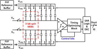 Similar content being viewed by others A 6-Bit Low Power SAR ADC High Performance SAR ADC with Mismatch Correction Latch and Improved Comparator Clock High Energy Efficiency and Linearity Switching Scheme Without Reset Energy for SAR ADCY. Cao, Y. Chen, Z. Ni, F. Ye, J. Ren, An 11b 80 ms/s SAR ADC with speed-enhanced SAR logic and high-linearity CDAC. In: 2018 IEEE Asia Pacific Conference on Circuits and Systems (APCCAS), pp. 18–21 (2018) Y. Chen, J. Wang, H. Hu, F. Ye, J. Ren, A 200 ms/s, 11 bit SAR-assisted pipeline ADC with bias-enhanced ring amplifier. In: 2017 IEEE International Symposium on Circuits and Systems (ISCAS), pp. 1–4 (2017) Y. Chen, X. Zhu, H. Tamura, M. Kibune, Y. Tomita, T. Hamada, M. Yoshioka, K. Ishikawa, T. Takayama, J. Ogawa, S. Tsukamoto, T. Kuroda, Split capacitor DAC mismatch calibration in successive approximation ADC. In: 2009 IEEE Custom Integrated Circuits Conference, pp. 279–282 (2009) Y. Chung, C. Yen, An 11-bit 100-ms/s subranged-SAR ADC in 65-nm cmos. IEEE Trans. Very Large Scale Integr. (VLSI) Syst. 25 (12), 3434–3443 (2017) Article Google Scholar Y. Chung, C. Yen, P. Tsai, B. Chen, A 12-bit 40-ms/s SAR ADC with a fast-binary-window DAC switching scheme. IEEE Trans. Very Large Scale Integr. (VLSI) Syst. 26 (10), 1989–1998 (2018) B.P. Ginsburg, A.P. Chandrakasan, 500-ms/s 5-bit ADC in 65-nm CMOS with split capacitor array DAC. IEEE J. Solid-State Circuits 42 (4), 739–747 (2007) P. Harikumar, J.J. Wikner, Design of a reference voltage buffer for a 10-bit 50 ms/s SAR ADC in 65 nm CMOS. In: 2015 IEEE International Symposium on Circuits and Systems (ISCAS), pp. 249–252 (2015) M. Hesener, T. Eicher, A. Hanneberg, D. Herbison, F. Kuttner, H. Wenske, A 14b 40 ms/s redundant SAR ADC with 480 mhz clock in 0.13 pm CMOS. In: 2007 IEEE International Solid-State Circuits Conference. Digest of Technical Papers, pp. 248–600 (2007) C. Hsu, S. Chang, C. Huang, L. Chang, Y. Shyu, C. Hou, H. Tseng, C. Kung, H. Hu, A 12-b 40-ms/s calibration-free SAR ADC. IEEE Trans. Circuits Syst. I: Regular Papers 65 (3), 881–890 (2018) Y. Hu, A. Liu, B. Li, Z. Wu, Closed-loop charge recycling switching scheme for SAR ADC. Electron. Lett. 53 (2), 66–68 (2017) G. Huang, S. Chang, Y. Lin, C. Liu, C. Huang, A 10b 200 ms/s 0.82 mw SAR ADC in 40 nm CMOS. In: 2013 IEEE Asian Solid-State Circuits Conference (A-SSCC), pp. 289–292 (2013) J.E. Kim, T. Yoo, K. Baek, T.T. Kim, Balanced sampling switch for high linearity and a wide temperature range in low power SAR ADCs. Electron. Lett. 55 (24), 1273–1275 (2019) D. Li, Z. Zhu, R. Ding, Y. Yang, A 1.4-mw 10-bit 150-ms/s SAR ADC with nonbinary split capacitive DAC in 65-nm CMOS. IEEE Trans. Circuits and Syst. II: Exp. Br. 65 (11), 1524–1528 (2018) W. Li, F. Li, J. Liu, H. Li, Z. Wang, A 13-bit 160 ms/s pipelined subranging-SAR ADC with low-offset dynamic comparator. In: 2017 IEEE Asian Solid-State Circuits Conference (A-SSCC), pp. 225–228 (2017) C. Liu, S. Chang, G. Huang, Y. Lin, A 10-bit 50-ms/s SAR ADC with a monotonic capacitor switching procedure. IEEE J. Solid-State Circuits 45 (4), 731–740 (2010) C. Liu, S. Chang, G. Huang, Y. Lin, C. Huang, C. Huang, L. Bu, C. Tsai, A 10b 100 ms/s 1.13 mw SAR ADC with binary-scaled error compensation. In: 2010 IEEE International Solid-State Circuits Conference—(ISSCC), pp. 386–387 (2010) C. Liu, C. Kuo, Y. Lin, A 10 bit 320 ms/s low-cost SAR ADC for IEEE 802.11ac applications in 20 nm CMOS. IEEE J. Solid-State Circuits 50 (11), 2645–2654 (2015) M. Liu, A. van Roermund, P. Harpe, A 7.1fj/conv.-step 88 db-sfdr 12b SAR ADC with energy-efficient swap-to-reset. In: ESSCIRC Conference 2016: 42nd European Solid-State Circuits Conference, pp. 409–412 (2016) M. Liu, A.H.M. van Roermund, P. Harpe, A 7.1-fj/conversion-step 88-db SFDR SAR ADC with energy-free swap to reset. IEEE J Solid-State Circuits 52 (11), 2979–2990 (2017) W. Liu, P. Huang, Y. Chiu, A 12b 22.5/45 ms/s 3.0 mw 0.059 mm2 CMOS SAR ADC achieving over 90 db SFDR. In: 2010 IEEE International Solid-State Circuits Conference-(ISSCC), pp. 380–381 (2010) M. Akbari, O. Hashemipour, F. Khateb, F. Moradi, An energy-efficient DAC switching algorithm based on charge recycling method for SAR ADCs. Microelectron. J. 82 , 29–35 (2018) M. Akbari, O. Hashemipour, M. Nazari, F. Moradi, A charge sharing-based switching scheme for SAR ADCs. Int. J. Circuit Theory Appl. 47 (7), 1188–1198 (2019) T. Miki, T. Morie, K. Matsukawa, Y. Bando, T. Okumoto, K. Obata, S. Sakiyama, S. Dosho, A 4.2 mw 50 ms/s 13 bit CMOS SAR ADC with SNR and SFDR enhancement techniques. IEEE J. Solid-State Circuits 50 (6), 1372–1381 (2015) C. Park, T. Chen, K. Noh, D. Zhou, S. Prakash, M.N. Alizadeh, A.I. Karsilayan, D. Chen, R.L. Geiger, J. Silva-Martinez, A 12-bit 125-ms/s 25-bit/cycle SAR-based pipeline ADC employing a self-biased gain boosting amplifier. IEEE Trans. Circuits Syst. I: Regular Pap. 67 , 1–12 (2020) Article MathSciNet Google Scholar J. Park, D. Kim, T. An, M. Kim, G. Ahn, S. Lee, 12 b 50 ms/s 0.18 \(\mu \) m CMOS SAR ADC based on highly linear C-R hybrid DAC. Electron. Lett. 56 (3), 119–121 (2020) Y. Roh, D. Chang, S. Ryu, A 40-nm cmos 12b 120-ms/s nonbinary SAR-assisted SAR ADC with double clock-rate coarse decision. IEEE Trans. Circuits Syst. II: Exp. Br. 67 (12), 1 (2020) Y. Shen, Z. Zhu, S. Liu, Y. Yang, A reconfigurable 10-to-12-b 80-to-20-ms/s bandwidth scalable SAR ADC. IEEE Trans. Circuits Syst. I: Regular Pap. 65 (1), 51–60 (2018) L. Sun, B. Li, A.K.Y. Wong, W.T. Ng, K.P. Pun, A charge recycling sar adc with a LSB-down switching scheme. IEEE Trans. Circuits Syst. I: Regular Pap. 62 (2), 356–365 (2015) W. Tseng, W. Lee, C. Huang, P. Chiu, A 12-bit 104 ms/s sar adc in 28 nm cmos for digitally-assisted wireless transmitters. IEEE J. Solid-State Circuits 51 (10), 2222–2231 (2016) W. Tung, S. Huang, An energy-efficient 11-bit 10-ms/s SAR ADC with monotonie switching split capacitor array. In: 2018 IEEE International Symposium on Circuits and Systems (ISCAS), pp. 1–5 (2018) D. Xu, H. Jiang, L. Qiu, X. Yu, J. Wang, Z. Zhang, C. Zhu, S. Xu, A linearity-enhanced 10-bit 160-ms/s SAR ADC with low-noise comparator technique. IEEE Trans Very Large Scale Integr (VLSI) Syst 27 (9), 1990–1997 (2019) J. Xue, H. Ghaedrahmati, J. Jin, A 10-bit 160ms/s SAR ADC with fast-response reference voltage buffer. In: 2018 14th IEEE International Conference on Solid-State and Integrated Circuit Technology (ICSICT), pp. 1–3 (2018) T. Yousefi, A. Dabbaghian, M. Yavari, An energy-efficient DAC switching method for SAR ADCs. IEEE Trans. Circuits Syst. II: Exp. Br. 65 (1), 41–45 (2018) H. Zhang, J. Sun, J. Zhang, R. Zhang, A. ChanCarusone, A low-power pipelined-SAR ADC using boosted bucket-brigade device for residue charge processing. IEEE Trans. Very Large Scale Integr. (VLSI) Syst. 26 (9), 1763–1776 (2018) M. Zhang, K. Noh, X. Fan, E. Sánchez-Sinencio, A 0.8–1.2 v 10–50 ms/s 13-bit subranging pipelined-sar adc using a temperature-insensitive time-based amplifier. IEEE J. Solid-State Circuits 52 (11), 2991–3005 (2017) Y. Zhu, C. Chan, U. Chio, S. Sin, U. Seng-Pan, R.P. Martins, F. Maloberti, A 10-bit 100-ms/s reference-free SAR ADC in 90 nm CMOS. IEEE J. Solid-State Circuits 45 (6), 1111–1121 (2010) Download references AcknowledgementsWe would like to thank the Chinese National Nature Science Foundation (No. 61974092) for funding this research. Chinese National Nature Science Foundation (No. 61974092) Author informationAuthors and affiliations. Center for Analog/RF Integrated Circuits (CARFIC), Department of Micro/Nano Electronics, Shanghai Jiao Tong University, Shanghai, 200240, China Mengying Hu, Jing Jin, Yuekang Guo, Xiaoming Liu & Jianjun Zhou You can also search for this author in PubMed Google Scholar Corresponding authorCorrespondence to Jing Jin . Ethics declarationsConflicts of interest/competing interests. No conflicts or interests with any authorities or person Availability of data and materialAll data used in this essay are collected by the authors mentioned in the essay without other sources Code availabilityNo software application or custom code are utilized in the research process Additional informationPublisher's note. Springer Nature remains neutral with regard to jurisdictional claims in published maps and institutional affiliations. Rights and permissionsReprints and permissions About this articleHu, M., Jin, J., Guo, Y. et al. A Power-Efficient SAR ADC with Optimized Timing-Redistribution Asynchronous SAR Logic in 40-nm CMOS. Circuits Syst Signal Process 40 , 3125–3142 (2021). https://doi.org/10.1007/s00034-020-01643-z Download citation Received : 03 August 2020 Revised : 23 December 2020 Accepted : 24 December 2020 Published : 21 January 2021 Issue Date : July 2021 DOI : https://doi.org/10.1007/s00034-020-01643-z Share this articleAnyone you share the following link with will be able to read this content: Sorry, a shareable link is not currently available for this article. Provided by the Springer Nature SharedIt content-sharing initiative
A 17 MS/s SAR ADC with energy-efficient switching strategyNew citation alert added. This alert has been successfully added and will be sent to: You will be notified whenever a record that you have chosen has been cited. To manage your alert preferences, click on the button below. New Citation Alert!Please log in to your account Information & ContributorsBibliometrics & citations, view options.
RecommendationsA 3.66 μw 12-bit 1 ms/s sar adc with mismatch and offset foreground calibration. This paper presents a 12-bit 1 MS/s successive approximation register (SAR) analog-to-digital converter (ADC) with foreground calibration for digital-to-analog converter (DAC) mismatch and comparator static offset errors. The proposed ... A 15-Bit 85 MS/s Hybrid Flash-SAR ADC in 90-nm CMOSA 15-bit, 85 MS/s hybrid flash-SAR ADC is presented. The proposed design combines modified tri-level switching technique with split capacitor technique to improve the power efficiency and sampling rate of the SAR block. The sampling switch was designed ... A 1.2 V 8-bit 1 MS/s SAR ADC with Res---Cap segment DAC for temperature sensor in LTEA 1.2 V 8-bit single ended successive approximation register analog-to-digital converter (ADC) for long term evolution (LTE) system is implemented. A novel 5-bit resistor and 3-bit capacitor segment digital-to-analog converter is used to minimize the ... InformationPublished in. Kluwer Academic Publishers United States Publication HistoryAuthor tags.
ContributorsOther metrics, bibliometrics, article metrics.
View optionsLogin options. Check if you have access through your login credentials or your institution to get full access on this article. Full AccessShare this publication link. Copying failed. Share on social mediaAffiliations, export citations.
We are preparing your search results for download ... We will inform you here when the file is ready. Your file of search results citations is now ready. Your search export query has expired. Please try again. IEEE Account
Purchase Details
Profile Information
A not-for-profit organization, IEEE is the world's largest technical professional organization dedicated to advancing technology for the benefit of humanity. © Copyright 2024 IEEE - All rights reserved. Use of this web site signifies your agreement to the terms and conditions. Information
InitiativesYou are accessing a machine-readable page. In order to be human-readable, please install an RSS reader. All articles published by MDPI are made immediately available worldwide under an open access license. No special permission is required to reuse all or part of the article published by MDPI, including figures and tables. For articles published under an open access Creative Common CC BY license, any part of the article may be reused without permission provided that the original article is clearly cited. For more information, please refer to https://www.mdpi.com/openaccess . Feature papers represent the most advanced research with significant potential for high impact in the field. A Feature Paper should be a substantial original Article that involves several techniques or approaches, provides an outlook for future research directions and describes possible research applications. Feature papers are submitted upon individual invitation or recommendation by the scientific editors and must receive positive feedback from the reviewers. Editor’s Choice articles are based on recommendations by the scientific editors of MDPI journals from around the world. Editors select a small number of articles recently published in the journal that they believe will be particularly interesting to readers, or important in the respective research area. The aim is to provide a snapshot of some of the most exciting work published in the various research areas of the journal. Original Submission Date Received: .
Article Menu
Find support for a specific problem in the support section of our website. Please let us know what you think of our products and services. Visit our dedicated information section to learn more about MDPI. JSmol ViewerAnalysis of the second-order ns sar adc performance enhancement based on active gain.  1. Introduction2. mathematical analysis of previous second-order fully-passive ns sar adc, 3. the proposed second-order ns sar adc, 3.1. the second-order ns sar adc based on active gain, 3.2. improved second-order ns sar adc based on active gain, 3.3. the values of a and δt/τ, 3.4. improved sampling speed, 3.5. kickback noise, 4. performance comparison, 5. conclusions, author contributions, data availability statement, conflicts of interest.
Click here to enlarge figure
Share and CiteJia, S.; Ye, T.; Xiao, S. Analysis of the Second-Order NS SAR ADC Performance Enhancement Based on Active Gain. Electronics 2024 , 13 , 3400. https://doi.org/10.3390/electronics13173400 Jia S, Ye T, Xiao S. Analysis of the Second-Order NS SAR ADC Performance Enhancement Based on Active Gain. Electronics . 2024; 13(17):3400. https://doi.org/10.3390/electronics13173400 Jia, Shichao, Tianchun Ye, and Shimao Xiao. 2024. "Analysis of the Second-Order NS SAR ADC Performance Enhancement Based on Active Gain" Electronics 13, no. 17: 3400. https://doi.org/10.3390/electronics13173400 Article MetricsArticle access statistics, further information, mdpi initiatives, follow mdpi. Subscribe to receive issue release notifications and newsletters from MDPI journals | ||||||||||||||||||||||||||||||||||||||||||
IMAGES
VIDEO
COMMENTS
AR ADC was designed and fabricated as a proof of concept for these design techniques.Finally, we investigated the concept of SAR-pipelining as a viable option to realize moderate. o high resolution (> 65 dB SNDR), high-speed (> 150 MS/s), low energy A/D converters. A mod.
The top-level block diagram of the asynchronous SAR ADC is shown below, along with the timing diagram of the important signals. ... "A study of SAR ADC and implementation of 10-bit asynchronous design," M.S. Thesis, Department of Electrical and Computer Engineering, University of Texas at Austin, 2013. [2] P. J. A. Harpe et al., "A 26 uW 8 bit ...
In this work, an asynchronous implementation of the SAR ADC was employed. Typical synchronous implementations [] make use of two synchronized clock sources, one to control the data sampling (the sampling clock) and other to control the converter iterations (the SAR iteration clock).On the other hand, asynchronous SAR ADCs [7, 8] require only one clock signal to control the sampling.
step FoM. This ADC achieves the best FoM of any ADCs with greater than 10b ENOB and 10MS/s sampling rate. Thesis Supervisor: Duane S. Boning Title: Professor of Electrical Engineering and Computer Science Thesis Supervisor: Hae-Seung Lee Title: Professor of Electrical Engineering and Computer Science 3
The proposed ADC is aimed at a tactile sensor application, requiring a low-noise and low-power solution. In addition, it should have high SNDR to detect even the weakest signals with precision. This thesis presents a 12-bit 400 kS/s SAR ADC implemented in a 180 nm CMOS technology for such a task.
ADC. ThesisPDF Available. Masters Dissertation: Design of a low-power 10-bit 12-MS/s asynchronous SAR ADC. September 2020. DOI: 10.11606/D.18.2020.tde-16122021-162821. Thesis for: Master of ...
A 150-MS/s 8-bit LU-SAR ADC is fabricated in a 130-nm CMOS technology to validate the concept. The measured result shows that the calibration improves the SNDR from 33.7-dB to 42.9-dB. The ADC consumes 640 μW from a 1.2 V supply with a Figure-of-Merit (FoM) of 37.5-fJ/conv-step. Moreover, the bit-wise impact of comparator noise is studied for ...
This paper presents a cutting-edge 1.2V 10-bit asynchronous Successive Approximation Register (SAR) Analog-to-Digital Converter (ADC) meticulously designed and simulated in the advanced 18 nm FinFET CMOS technology. This asynchronous SAR ADC system consists of an internal-clock generator, switching unit, fully differential pair of capacitive Digital-to-Analog Converter (DAC), a dynamic ...
Key words: SAR ADC, asynchronous SAR logic, bootstrapped switch, dynamic comparator, LHAASO, WCDA PACS: 84.30.-r, 07.05.Hd 1 Introduction The Large High Altitude Air Shower Observatory (LHAASO) project has been proposed for high energy gamma ray and cosmic ray detection [1-3]. One of the major components is the Water Cherenkov Detector Array
This paper introduces an innovative concept centered on developing an 8-bit Asynchronous Successive Approximation Register (SAR) Analog to Digital Converter (ADC) utilizing state-of-the-art 18nm FinFET technology. This advanced asynchronous SAR system encompasses multiple crucial components, including a precisely engineered internal clock generator, a high-performance bootstrapped sample and ...
A low power 12-bit, 20 MS/s asynchronously controlled successive approximation register (SAR) analog-to-digital converter (ADC) to be used in wireless access for vehicular environment (WAVE) intelligent transportation system (ITS) sensor based application is presented in this paper. To optimize the architecture with respect to power consumption and performance, several techniques are proposed.
D. Zhang, Design of Ultra-Low-Power Analog-to-Digital Converters, Linköping: PhD Thesis, 2012. Google Scholar; A. M. Abo and P. R. Gray, "A 1.5-V, ... Design of a low power 10-bit 12MS/s asynchronous SAR ADC in 65nm CMOS. Hardware. Integrated circuits. Very large scale integration design. Analog and mixed-signal circuits.
Successive approximation register (SAR) analog-to-digital converters (ADCs) are widely used in biomedical and portable/wearable electronic systems due to their excellent power efficiency. However, both the design and the optimization of high-performance SAR ADCs are time consuming, even for well-experienced circuit designers. For system designers, it is also hard to quickly evaluate the ...
1.1 Thesis organization 3 2. High-speed sampling 4 2.1 Track-and-hold circuits 4 ... asynchronous SAR ADC with 400mV input swing and 1.05V supply 34 3.8 Waveform of a classic asynchronous SAR ADC in the scenario that (a) a meta-stability event does not cause a sparkle-code and (b) a meta-stability event caused a sparkle-code 35 ...
A 26 $\mu$ W 8 bit 10 MS/s Asynchronous SAR ADC for Low Energy Radios. The fully dynamic design, which is optimized for low-leakage, leads to a standby power consumption of 6 nW and the energy efficiency of this converter can be maintained down to very low sampling rates.
A loop-unrolled asynchronous SAR ADC is used to speed up the sub-ADC further. This architecture uses n comparators for an n-bit ADC. The outputs of the comparators can be directly given to the SAR DAC array without any extra logic and there is also no need for the comparators to do the reset within one conversion period. ... Thesis (Ph.D ...
A design of low-power 10-bit 1 MS/s asynchronous successive approximation register analog-to-digital converter (SAR ADC) is presented in this paper. To improve the linearity of the digital-to-analog converter (DAC) and energy efficiency, a common mode-based monotonic charge recovery (CMMC) switching technique is proposed. The proposed switching technique consumes only 63.75 CVREF2 switching ...
First, a 9-bit 16-way time-interleaved SAR ADC core including decoupling capacitor and voltage references are fully generated by the generator. It works at sampling rate 10GS/s and simulated SNDR is 37.6 dB at Nyquist frequency. In order to set the con guration bits and read out quantized result.
This paper presents a comparison between a Itl-bit asynchronous SAR (ASAR) ADC and a 10-bit synchronous SAR (SSAR) ADC, both designed and simulated in a 22-nm FDSOI CMOS process. To further support the simulation results, the ASAR ADC has also been fabricated and measurements are pre-sented. As opposed to the abrupt SNDR collapse in the SSAR ADC, the SNDR of the ASAR ADC shows a more graceful ...
Low-power, high-speed ADCs are in great needs. New opportunities and breakthroughs are expected in accelerated rate. Asynchronous SAR ADC architecture provides power efficient platform for achieving this goal. The record high-speed (90GS/s) ADC also leverages this topology.
This paper presents a power-efficient successive-approximation register (SAR) analog-to-digital converter (ADC) with fast response reference buffer (RV-buffer). Several techniques are applied in the system design to improve the performance of the SAR ADC. A novel timing-redistribution SAR logic is proposed to balance the difference between required settling time for the most significant bit ...
This work presents the design and implementation of a low power successive approximation register analog-to-digital converter (SAR ADC) in a 65nm CMOS technology, suitable for low power frontend of wireless receivers with a flexible sampling rate up to 12 MS/s.
A study of SAR ADC and implementation of 10-Bit asynchronous design. A thesis submitted to the University of Texas at Austin for the degree of Master of Science in Engineering. ... Wen, J. Y., Chang, P. H., Huang, J. F., & Lai, W. C. (2015). Chip design of a 12-bit 5MS/s fully differential SAR ADC with resistor-capacitor array DAC technique for ...
In this paper 8 bit SAR ADC with input voltage of 1.2V has been designed. The schematic diagram of different sub blocks has been implemented in Cadence Virtuoso using 180nm technology. Comparator was designed so that it remains in saturation for proper operation and was implemented using differential amplifier. The comparator is the main power consuming block, so most of our effort was focused ...
This paper presents a novel second-order passive noise shaping (NS) successive approximation register (SAR) analog-to-digital converter (ADC) based on active gain. The proposed scheme achieves a further improvement in the signal-to-noise ratio (SNR) of the proposed NS SAR ADC by reducing the kT/C noise and the conversion rate. After having presented the conversion principle, the theoretical ...